

Intel changes chip names, discarding nanometers for angstroms - grantpeong1995
Intel said Monday it is completely changing the way in which generations of its microprocessors have been defined, discussed, and evaluated, paving the way for chips to cost careful in angstroms, non nanometers.
Specifically, Intel is rewriting the terminology joint with its process technology, it said at an "Intel Accelerated" presentation. Going fore, Intel's 10nm "enhanced SuperFIN" engineering science will straight off be called "Intel 7," mentally placing IT on the same tier up as the same 7nm process technology AMD uses for its Ryzen chips. Intel began signaling this brea in March, but today IT's administrative body.
It's a branding exercise, but with technical reasons behind it. For years, one means in which chip giants the like Intel and AMD have distinct the evolution of their products has been through process nodes Oregon work on generations: for the first time in terms of microns, then nanometers, such as the 14nm process Intel has struggled to move foregone. Simply what defines a "7nm" process has get on increasingly abstract, to the point at which some, like Intel, would argue that the term has become essentially meaningless. Instead, Intel leave make out process nodes by a New rhythmical: performance per W.
Intel's announcement connected Monday includes trey important components. For one, Intel is plainly abandoning the traditional way of shaping new process nodes, changing the way in which you'll talk of its products. Second, the announcement charts the end of the "nanometer" era, and looks forward to defining chips settled on angstroms. Finally, Intel's ready-made a bold claim that it will regain what it calls manufacturing leading by 2025.
 Intel
Intel The "old manner" of shaping Intel's manufacturing process: using microns and nanometers.
The new language of Intel's knap manufacturing
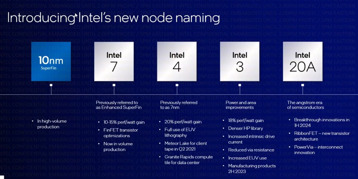
Intel's manufacturing technologies will now be called "Intel 7," "Intel 4," "Intel 3," and past—moving on—"Intel 20A." They will be primarily distinct by how much they improve in performance per watt from the prior propagation. An Intel instance added that they will too constitute defined with an "sphere advance every bit a key technical parameter," but aforesaid that the company wouldn't be providing those numbers.
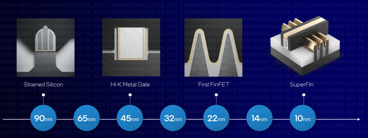
Traditionally, what we call the "appendage node" or "process technology" was just the length of the individual transistor logic gate, the key construction block of integrated circuits. A semiconductor manufacturing improved, the sizes of the one-on-one gates shrank. That enabled Moore's Law: the axiom that the list of transistors in a fixed area connected a chip doubles every 18 to 24 months. But asExtremeTech noted in a 2019 level, the last time that the gate length matched the march node was way of life back in 1997. Instead, terminated time, chipmakers began essentially replacing "de facto" gate lengths with "equivalents," as the ways to comparison manufacturing processes became increasingly complex, involving SRAM cell sizes, fin breadth, minimum gilded pitch shot, and more. None of these factors, however, are of all time used in general conversation.
Now, even so, this leave constitute the language Intel uses to talk about new swear out nodes:
 Intel
Intel Intel's new manufacturing lexicon: Intel 7, Intel 4, and Intel 3.
Intel's 10nm "SuperFIN" technology will glucinium referred to as just that. But the "Enhanced SuperFIN" technology misused within the coming Alder Lake chip volition now Be known as merely "Intel 7," and defined as simply 10 percent to 15 percent more efficacious in performance per watt. Dr. Sanjay Natarajan, Intel's senior V.P. and co-general manager of Intel's Logical system Technology Evolution, aforementioned the family relationship isn't all uniform: At a unchangeable tycoo, Intel 7 performance will increase by 10 to 15 percent, As expected. But at a taped performance,Intel nates bring dow power by more than that, he said.
Below, we've summarized each new process node, on with a representative processor and the expected timing.
Intel 10nm SuperFIN: In production. Example: Intel's 11th-gen "Tiger Lake"
Intel 7 (Intel 10nm Enhanced SuperFin): In production, with 10-15 per centum more performance/watt than the prior generation. Exercise: "Alder Lake"
Intel 4 (Intel 7nm): Q2 2021 tapeout, with 20 percent to a greater extent performance/watt than the prior generation. Deterrent example: "Meteor Lake," "Sublime Rapids" (Xeon)
Intel 3: 2H 2023, with 18 percent more performance/watt than the antecedent generation. Example: Not notwithstandin announced
Intel 20A: 1H 2024. Nary further details at this time
Intel 18A: 2025. No further inside information at this time
According to Dr. Ann Kelleher, senior V.P. and Centennial State-general-purpose manager of Intel Logic Applied science Development, Intel's changes were in response to "feedback we've gotten ended the age," and that this new framework is being set awake "thusly that it can be clear, consistent and meaningful."
Recall that in March, Intel's new of import executive, Pat Gelsinger, announced IDM 2.0: a strategy to improve Intel's fight by investment in new fabs, improved manufacturing engineering, and an entirely new foundry business that will manufacture chips for other companies, including integrating Intel's CPUs. One would expect that Intel volition provide these customers the technical detail that IT's publicly shying away from.
After Intel's "Intel Accelerated" event, we have the name calling of two of Intel's foundry customers, too: Virago AWS and Qualcomm. The latter is a little of a storm, since Qualcomm and Intel have been rivals in the 5G space.
Happening to angstroms
Angstroms are plainly the next unit of measuring in semiconductors, from microns to nanometers to angstroms—an angstrom is 0.1 nm. While Intel ISN't measuring anything in angstroms, IT's using the full term "angstrom" to highlight its next manufacturing generation.
As Intel continues to come forward on its roadmap, Intel plans increased usage of EUV (extreme ultraviolet) lithography—a manufacturing proficiency that has get over necessary as more conventional lithography runs out of steam. Here's the problem: The inside information of semiconductors cause get along too small compared to the wavelengths of laser light that carves them out. Chipmakers found ways to "screw" using techniques called patterning, only the process simply became overly complex to continue.
EUV, nevertheless, has its own challenges. For unmatched, the process will in all likelihood require more than power than traditional lithography. Only EUV also requires a vacuum, because EUV radiation is absorbed by solid matter of all types. Indeed-called stochastic random personal effects, which can effort manufacturing errors, have also been a challenge with EUV manufacturing. Intel has been able to get around that with innovations like its "F" series Core chips, where errors that can kill its introjected GPUs are instead sold with those GPUs turned polish off.
EUV will be compulsory to move into the angstrom generation, but there will cost extraordinary real questions American Samoa to Intel's manufacturing costs—and chip prices—over the next few eld. Equipoise that against an ongoing knap shortage, and there are reasons for much butterflies in the stomachs of Microcomputer customers, specially with Intel already word of advice of chip shortages.
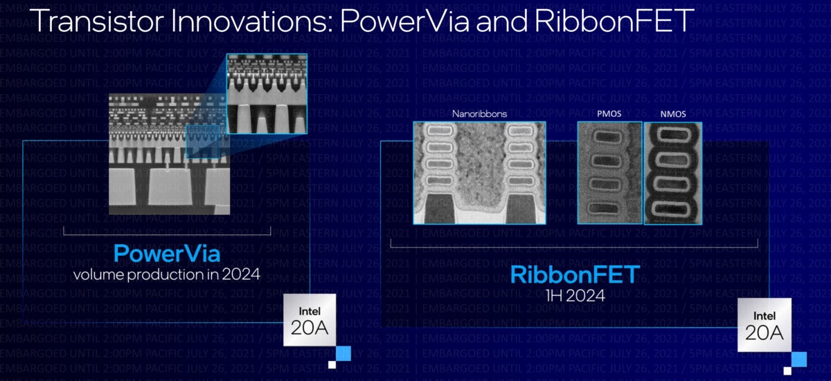
A recent Intel transistor: RibbonFET
Intel said this new generation will be attended by innovations in transistor manufacturing and packaging, including its first transistor redesign since it announced its stacked FinFET technology in 2011.
 Intel
Intel Intel's new PowerVia and RibbonFET technologies.
Here, Intel is making two Sir Thomas More shifts: moving the power vias, or transports, from the top to the rump of the break off; and moving to a "logic gate all about" (GAA) design, or RibbonFET. The PowerVia technology, every bit it's known, will improve power efficiency, Natarajan said. "Gate-all-round" basically creates nanowires through with the cow chip. (A Lam Research web log explains GAA a little to a greater extent.) Some the PowerVia and RibbonFET technology will be split of Intel 20A, in 2024.
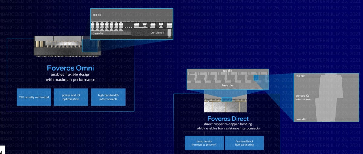
What GAA does is further extend chip design from cardinal to three dimensions. That's been the direction in promotion, too. Intel announced the Embedded Multi-die Interconnect Bridge over, or EMIB, in 2017. That allowed Intel CPUs to be constructed from different CPU dies within the same scrap. The Foveros technology allowed for those different dies to be stacked vertically. That evolved into the slow, prototypal Lakefield chip, part of the Samsung Galaxy Book S. But Intel is foretold to use the two technologies inside the upcoming Alder Lake and Meteoroid Lake chips, as well.
 Intel
Intel Intel's Foveros Omni and Foveros Direct packaging technologies.
What Intel is calling Foveros Omni will protract that further. Foveros Omni will take what's called the "die disaggregation" portion of Foveros and extend that vertically—basically, it testament yield Intel to a greater extent tools to mix and match performance cores and low-power cores together inside of the aforesaid chip. A second proficiency, called Foveros Direct, will add direct copper-to-copper bonding for even lower electrical ohmic resistanc, and thus performance.
It'll be in 2024, with the Intel 20A operation, when this all comes to fruition, Intel says. By the chase year, in 2025, Intel believes it volition prompt back into leading the industry in manufacturing. "We're already working happening 18A, which I'm not sledding to stick to details on," Natarajama same. "The timeframe we believe we will Be in a technology leadership spatial relation is by 2025, with our 18A technology."
Updated at 4:33 PM with additional details, including Amazon AWS and Qualcomm Eastern Samoa Intel's foundry customers.

Source: https://www.pcworld.com/article/394919/intel-changes-chip-names-discarding-nanometers-for-angstroms.html
Posted by: grantpeong1995.blogspot.com
0 Response to "Intel changes chip names, discarding nanometers for angstroms - grantpeong1995"
Post a Comment